


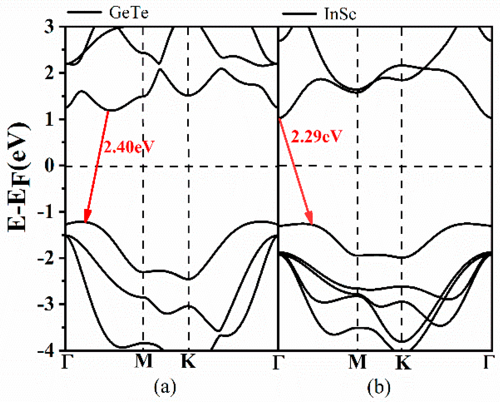
Nanomaterials Free Full Text The Electronic And Optical Properties Of Inse Gete Heterobilayer Via Applying Biaxial Strain Html

The Select A Fuzz Is A Pretty Interesting Fuzz Box From Foxx It Has A Rotary Switch To Select The Input Cap The Larger The Cap Th Fuzz Transistors Good Notes

Density Functional Theory Calculations Revealing Metal Like Band Structures And Work Function Variation For Ultrathin Gallium Arsenide 111 Surface Layers Tan 2019 Chemistry 8211 An Asian Journal Wiley Online Library

Transition Metal Perovskite Chalcogenide A New Class Of Highly Tunable Optoelectronic Semiconductors Optical Image Semiconductors Transition Metal


Germanium Outperforms Silicon In Energy Efficient Transistors With N Und P Conduction Transistors Conduction Energy Efficiency


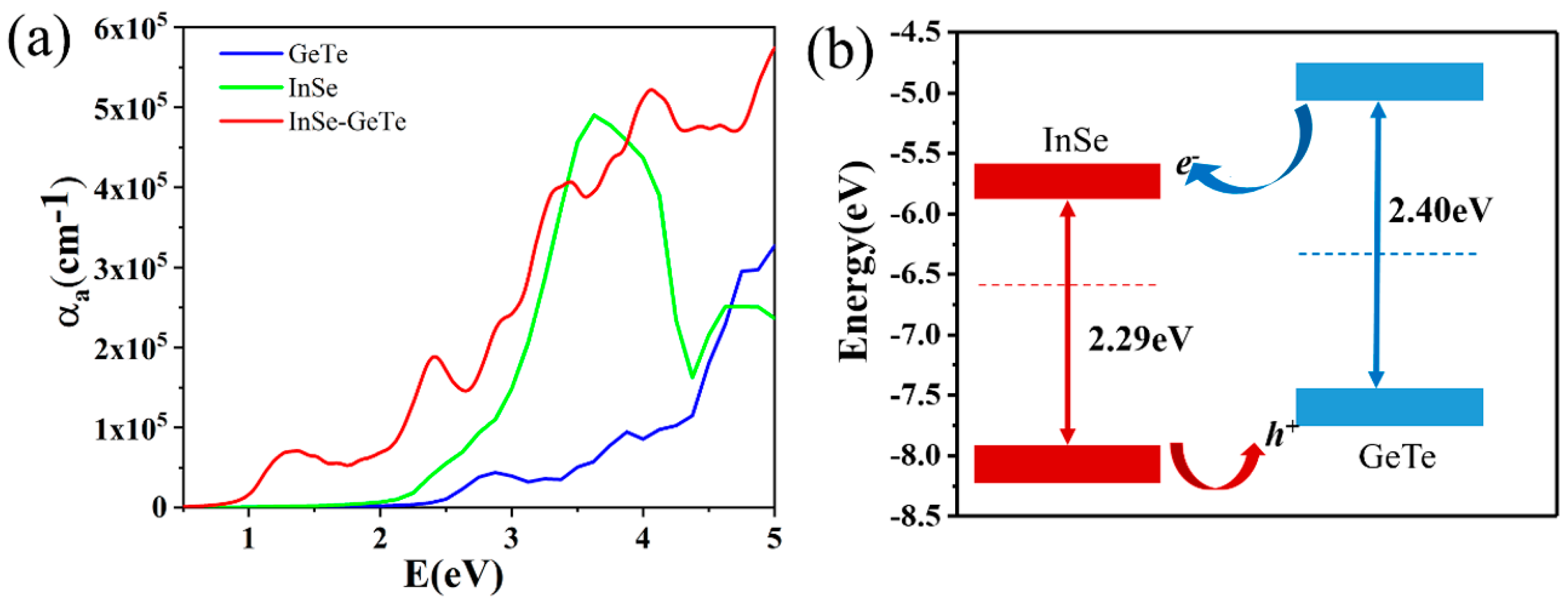
Nanomaterials Free Full Text The Electronic And Optical Properties Of Inse Gete Heterobilayer Via Applying Biaxial Strain Html


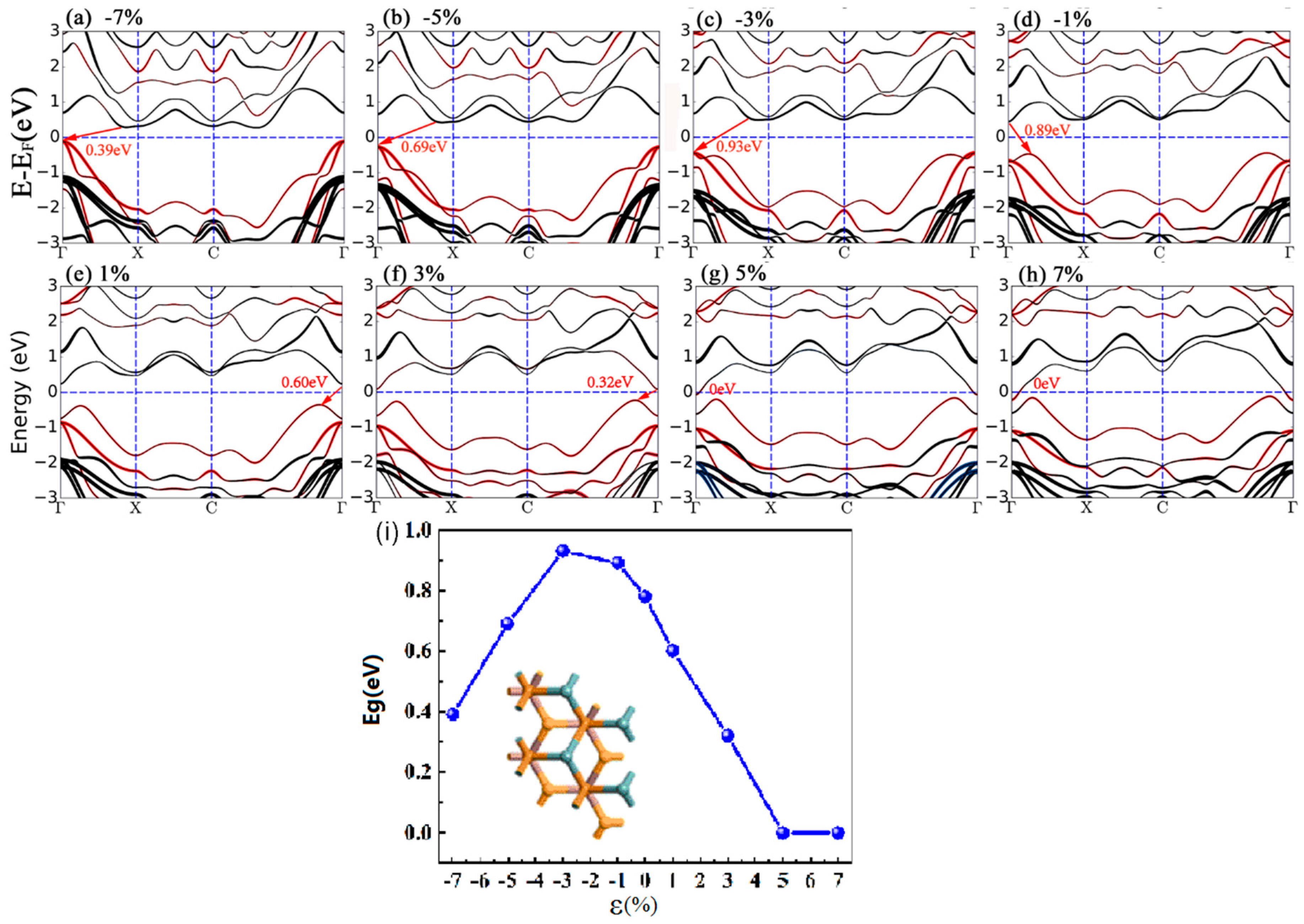
Nanomaterials Free Full Text The Electronic And Optical Properties Of Inse Gete Heterobilayer Via Applying Biaxial Strain Html


Http Www Electronicsandyou Com Blog How Semiconductor Works Html Semiconductor Semiconductor Technology Semiconductor Materials

Intrinsic Semiconductor Lattice Structure Holes Videos Solved Examples Semiconductor Intrinsic Simple Circuit
No comments:
Post a Comment